
APPLICATION NOTE
AT11493: Waveform Generator and WAV Audio Player
using DAC
ATSAMD20J18
Introduction
This application note explains the basics of Digital-to-Analog Converter (DAC)
and their application usage with two examples. The first example demonstrates
simple waveform generation using DAC and the second example demonstrates
an audio player playing .wav files stored in a microSD card.
For demonstration purpose Atmel
®
| SMART SAM D20 Xplained Pro board along
with IO1 Xplained Pro wing board will be used.
Atmel-42458A-Waveform-Generator-and-WAV-Audio-Player-using-DAC_ApplicationNote_042015

AT11493: Waveform Generator and WAV Audio Player using DAC [APPLICATION NOTE]
Atmel-42458A-Waveform-Generator-and-WAV-Audio-Player-using-DAC_ApplicationNote_042015
2
2
Table of Contents
1 Introduction on Digital-to-Analog Converter (DAC) .................................................. 3
2 DAC Implementation in SAM D MCUs ........................................................................ 4
2.2 DAC Registers ...................................................................................................................................... 4
2.3 DAC Reference ..................................................................................................................................... 5
2.4 DAC Conversion ................................................................................................................................... 5
3 Application Demonstration ......................................................................................... 6
3.1 Waveform Generator ............................................................................................................................. 6
3.1.2 Clock Flow ................................................................................................................................ 7
3.1.3 Getting Started ......................................................................................................................... 8
3.1.4 Application Limitations .............................................................................................................. 9
3.2 WAV Audio Player ................................................................................................................................. 9
3.2.2 Getting Started ....................................................................................................................... 12
3.2.3 Application Limitations ............................................................................................................ 14
4 References ................................................................................................................. 14
5 Revision History ........................................................................................................ 15
AT11493: Waveform Generator and WAV Audio Player using DAC [APPLICATION NOTE]
Atmel-42458A-Waveform-Generator-and-WAV-Audio-Player-using-DAC_ApplicationNote_042015
3
3
1 Introduction on Digital-to-Analog Converter (DAC)
Digital-to-Analog Converter (DAC) is a module that takes up digital code as input and converts them into
appropriate analog signal. DAC uses a reference voltage to convert the input digital code into output analog
voltage.
A DAC’s resolution is determined by the number of bits in the digital input code and the reference voltage
applied to the DAC. Typically the output voltage of a DAC is estimated by the following formula:
For example, for a 3-bit DAC with 2V reference voltage and digital input code as 101, the DAC output voltage
will be ~1.428V. The accuracy of a DAC module will be represented in terms of LSBs. An LSB value of a DAC
depends on reference voltage and number of bits in the digital input. An LSB calculation follows the following
formula:
So 1 LSB ~= 1.953mV for a 10-bit DAC with 2V reference.
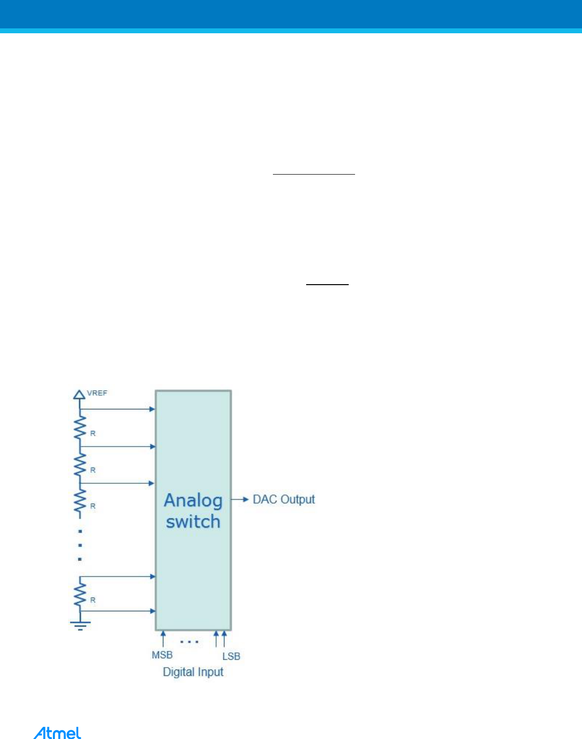
A simplified DAC implementation theoretically uses a resistor ladder network and an analog switching circuit as
shown in Figure 1-1.
Figure 1-1. Basic DAC Implementation
AT11493: Waveform Generator and WAV Audio Player using DAC [APPLICATION NOTE]
Atmel-42458A-Waveform-Generator-and-WAV-Audio-Player-using-DAC_ApplicationNote_042015
4
4
When the number of bits in the digital input code increases, the number of components in the above network
increases in terms of power of two which increases the DAC footprint in silicon. So the DAC implementation in
microcontrollers might not be the same as shown above. However the basic concept behind the DAC working
and the output calculation follows the above mentioned formula.
2 DAC Implementation in SAM D MCUs
The DAC module in SAM D microcontrollers has 10-bit resolution with single channel. The maximum sampling
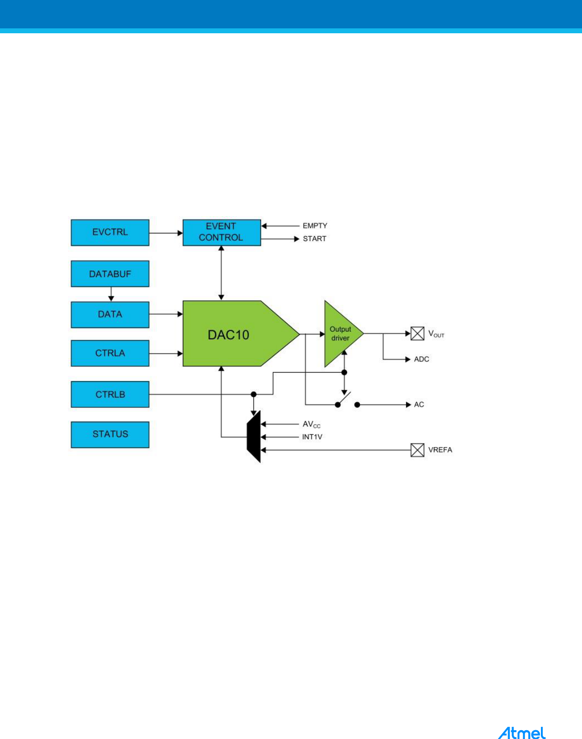
rate for the DAC in SAM D microcontrollers is 350ksps. Figure 2-1 provides the basic block diagram of the
DAC module.
Figure 2-1. SAM D20 DAC Block Diagram
2.2 DAC Registers
The DAC module has two data registers namely the DATA and DATABUF registers. The DATABUF register is
a buffer register mainly used with Event System. More details about the usage of these registers will be
covered in the upcoming section.
DAC module has two control registers, CTRLA and CTRLB which are used for configuring and enabling the
DAC module.
The CTRLA register has software reset bit (SWRST) which resets all the DAC registers, an ENABLE bit for
enabling/disabling the DAC module and run in standby (RUNSTDBY) bit for making the DAC module operate
during standby sleep mode (SleepWalking).
The CTRLB register has bits that control the DAC output, both external and internal, digital input data
adjustment bit, voltage pump disable bit, and reference selection bits.
The STATUS register has a synchronization busy flag (SYNCBUSY). In SAM D microcontrollers all peripherals
are supplied with two clocks. One peripheral bus clock (APB) used for accessing the peripheral registers and
one generic clock with which the peripheral actually operates. Registers that lie between these two clock
domains needs clock synchronization before it is read or written. In DAC module, registers like CTRLA, DATA,

AT11493: Waveform Generator and WAV Audio Player using DAC [APPLICATION NOTE]
Atmel-42458A-Waveform-Generator-and-WAV-Audio-Player-using-DAC_ApplicationNote_042015
5
5
and DATABUF registers are write-synchronized. This means that the application software should ensure that
the SYNCBUSY flag is not set before writing to these registers.
The EVCTRL register controls the input and output events to/from the DAC module. The DAC module supports
one event input and one event output. An input event can trigger a DAC conversion action upon reception. The
DAC module can generate an event output when the DAC data buffer is empty. More details on the event
mechanism will be covered in the upcoming section.
The DAC supports three interrupts which are configured through interrupt enable (INTENSET), interrupt
disable (INTENCLR), and interrupt flag (INTFLAG) registers. The interrupts are data buffer empty (EMPTY),
data buffer underrun (UNDERRUN), and synchronization ready (SYNCRDY). The EMPTY interrupt is triggered
when there is no data in the DATABUF register. The UNDERRUN interrupt is triggered when there is no data
in DATABUF register and if an input event occurs. The SYNCRDY interrupt is triggered when the register
synchronization in DAC module is finished.
2.3 DAC Reference
The DAC module in SAM D microcontrollers supports three different reference sources namely:
Internal 1V bandgap reference (INT1V)
AVcc reference (AVCC)
External reference voltage on I/O pin (VREFA)
The INT1V reference source is derived from the voltage reference system in the System Controller (SYSCTRL)
module. In order to use this voltage reference the BGOUTEN bit (Bandgap Output Enable) in VREF register in
SYSCTRL module has to be first set.
The AVcc reference is taken from the analog supply voltage AVCC = VDDANA.
The VREFA is the external voltage reference applied on an I/O pin. In SAM D20 devices, VREFA is alternate
function B on I/O pin PA03.
Note: The external voltage reference option has certain min/max limits. It should be minimum 1.0V and can
be maximum VDDANA – 0.6V. For example if VDDANA = 3.3V, then the maximum external reference
voltage that can be applied is 3.3V – 0.6V = 2.7V.
2.4 DAC Conversion
An input sample conversion in DAC can be either triggered by software or by other peripherals via event
system. Conversion through software is achieved by directly writing to the DATA register in the DAC module.
Writing a digital code to the DATA register will immediately start a conversion.
Event system based conversion is achieved by writing to the DATABUF register. Writing the digital code to the
DATABUF register will keep the data in buffer register and waits for an event to occur to start a conversion. If
the DAC is configured to start a conversion based on an input event and if a valid event happens through the
event channel then the data in the buffer register will be automatically transferred to DATA register and the
conversion is initiated.
Even though a conversion is initiated by an event from Event System, the application software has to write to
the DATABUF register. The advantage of using event based DAC conversion is the deterministic timing
between the output samples which is critical when audio playback or waveform generation is implemented.
The DAC conversion in SAM D microcontrollers follows the following formula.

AT11493: Waveform Generator and WAV Audio Player using DAC [APPLICATION NOTE]
Atmel-42458A-Waveform-Generator-and-WAV-Audio-Player-using-DAC_ApplicationNote_042015
6
6
Note: Even though the DAC output voltage theoretically follows the above equation, practically the linear
output conversion range is limited to certain min/max limits in SAM D microcontrollers. The linear
output voltage range for SAM D DAC is from 0.05V to (VDDANA – 0.05) V. This means that the DAC
module cannot guarantee proper output voltages below 0.05V and above VDDANA – 0.05V.
3 Application Demonstration
Two different applications have been implemented demonstrating the DAC module of SAM D20.
The first project demonstrates a simple waveform generator application with DAC and the second project
demonstrates a WAV audio player with DAC.
Chapter 3 explains the DAC example projects in detail with application flow and getting started steps. This
chapter assumes that user has previous knowledge on programming/debugging a SAM D20 device using
Atmel Studio IDE.
Following are the hardware requirements to test the waveform generator application and WAV audio player
application.
SAM D20 Xplained Pro board
I/O1 Xplained Pro wing board
Both the applications has been tested with Atmel Studio 6.2 with ASF version 3.21.0 and above.
3.1 Waveform Generator
The waveform generator is a basic application using the DAC module. In this application three waveforms (sine
wave, triangular wave, and saw-tooth wave) will be generated with configurable frequency. Along with DAC
module, Timer, and Event System will be used to accurately convert the input digital data into analog
waveform.
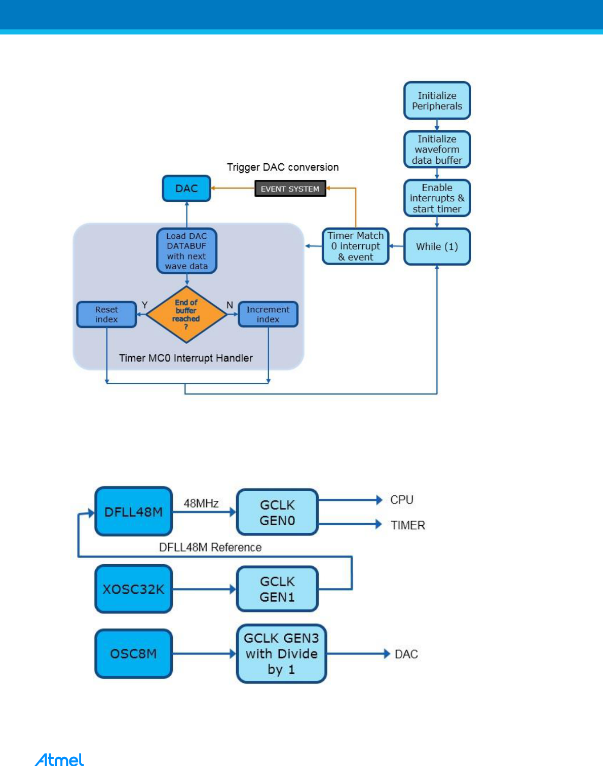
During initialization stage the application software fills up a buffer with the digital data corresponding to one
cycle of the selected waveform.
A timer is configured to operate in Match Frequency mode and the compare channel 0 is loaded with a value
corresponding to the configured frequency of the output waveform. Compare value to be loaded for a timer
channel is calculated as below:
The DAC module is configured to use internal 1V bandgap as reference and conversion triggered by an input
event from the event system.
An event channel is configured with event generator as timer match channel 0 and event user as DAC start
conversion.
Timer interrupt for compare match channel 0 is also enabled so that inside the timer interrupt handler the next
DAC data to convert is loaded from the waveform buffer into the DATABUF register. If the end of the buffer is
reached then the buffer index has to be reset so that the cycle continues again.
Note: When the timer channel 0 match occurs, both event and interrupt will be generated at the same time.
However the event action inside DAC will happen before the timer ISR is executed which ensures that
the old value in DATABUF is transmitted into DATA register by the event before ISR code writes a new
value into the DATABUF register.
The overall block schematic of the application looks as shown in Figure 3-1.
AT11493: Waveform Generator and WAV Audio Player using DAC [APPLICATION NOTE]
Atmel-42458A-Waveform-Generator-and-WAV-Audio-Player-using-DAC_ApplicationNote_042015
7
7
Figure 3-1. Application Flow Diagram – Waveform Generator
3.1.2 Clock Flow
The block diagram in Figure 3-2 depicts the clock system and its flow for this application.
Figure 3-2. Clock Flow Diagram – Waveform Generator
AT11493: Waveform Generator and WAV Audio Player using DAC [APPLICATION NOTE]
Atmel-42458A-Waveform-Generator-and-WAV-Audio-Player-using-DAC_ApplicationNote_042015
8
8
XOSC32K, OSC8M, and DFLL48M are the three clock sources used. GCLK Generator 1 is sourced by
XOSC32K which is provided as the reference clock for DFLL48M. DFLL48M is configured in closed loop mode
to generate a 48MHz clock which is given as clock source for GCLK Generator 0. The GCLK Generator 0
feeds the main clock domain (CPU, AHB, and APB buses) as well as the timer.
OSC8M is enabled and provided as the clock source for GCLK Generator 3 which feeds the DAC module after
a prescaling factor of one. So the effective clock that DAC receives is 8MHz.
3.1.3 Getting Started
Open the example project “DAC Waveform Generator – SAM D20 Xplained Pro” in ‘Atmel Studio → File →
New → Example Project”.
Open the file main.c under ‘src’ folder and modify the following macros which set the required waveform mode
and frequency of the output waveform.
#define WAVE_MODE SINE_WAVE
#define FREQUENCY_HZ 150
The other wave modes can be SAW_TOOTH_WAVE and TRIANGLE_WAVE.
Now save the file, right click on ‘Waveform_Generator’ and click ‘Build’ which builds the project. Start the
debug session and run the project.
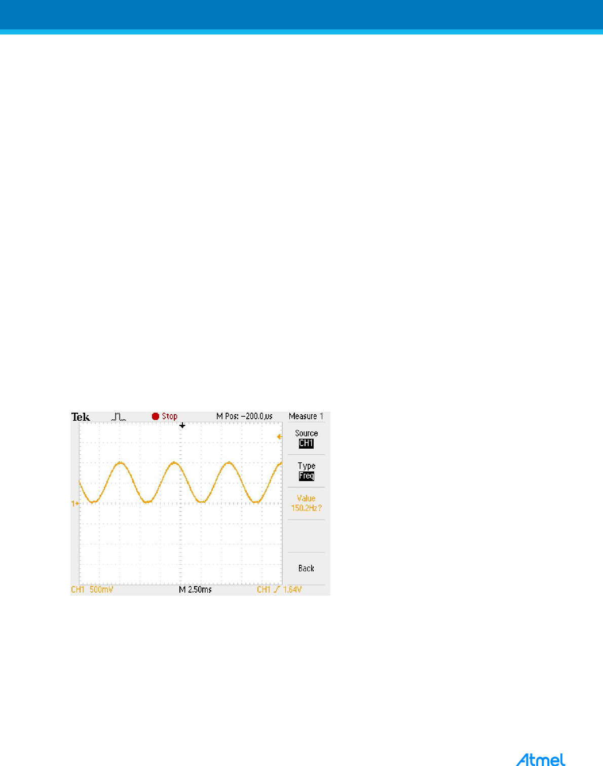
The waveform output can be probed on pin PA02 available on EXT3 header in SAM D20 Xplained Pro board.
Figure 3-3, Figure 3-4, and Figure 3-5 show the scope plots of the three waveform outputs (re-compiled and re-
programmed for each waveform).
Figure 3-3. Sine Wave Output – Scope-Shot
AT11493: Waveform Generator and WAV Audio Player using DAC [APPLICATION NOTE]
Atmel-42458A-Waveform-Generator-and-WAV-Audio-Player-using-DAC_ApplicationNote_042015
9
9
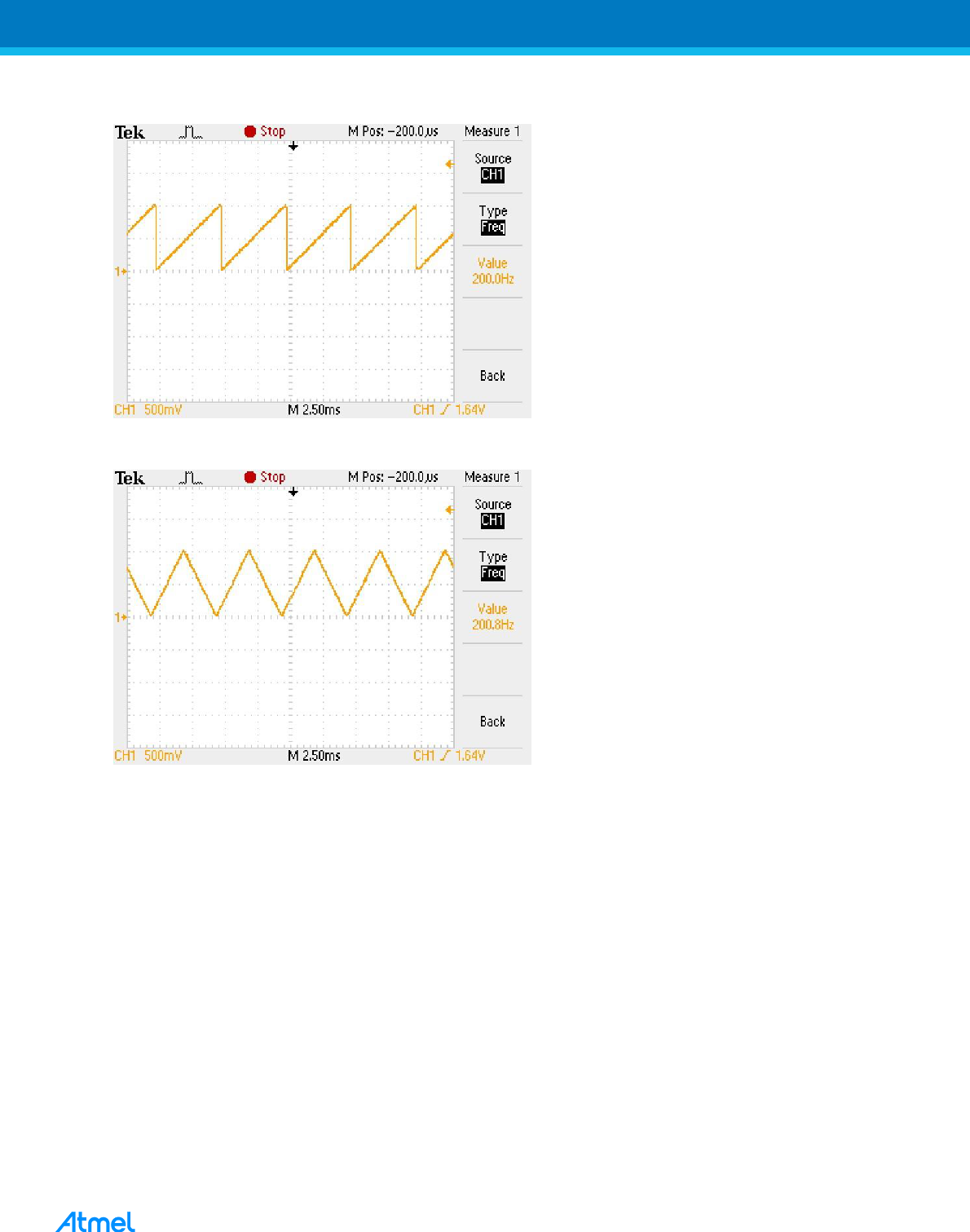
Figure 3-4. Saw-Tooth Wave Output – Scope-Shot
Figure 3-5. Triangular Wave Output – Scope-Shot
3.1.4 Application Limitations
The frequency of the output waveform is limited by the sampling rate of the DAC and the buffer size of the
waveform. For sine wave the maximum frequency for a 360 point data buffer at 350ksps is ~970Hz. For saw
tooth and triangular waves the maximum frequency for a 256 point data buffer at 350ksps is ~1.367kHz.
3.2 WAV Audio Player
The WAV audio player is an advanced application using the DAC module. This application plays audio files
with .wav extension stored in a microSD card.
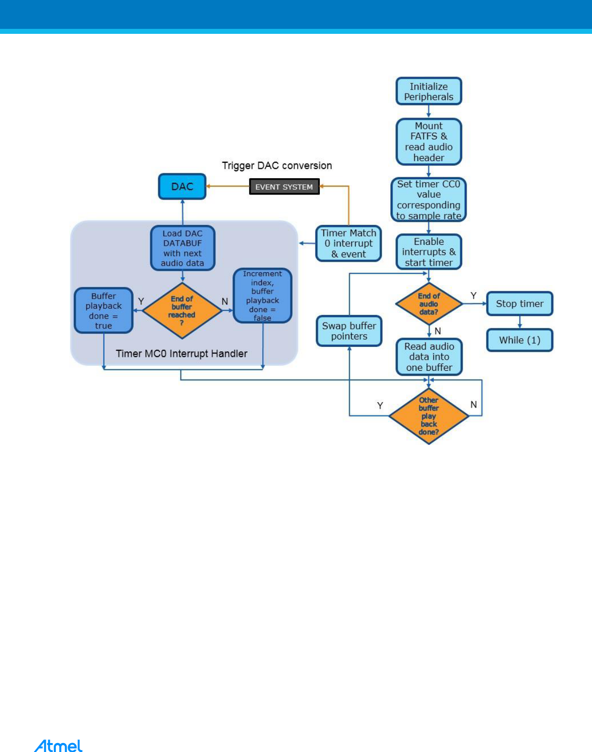
The application flow for WAV audio player follows the same flow as waveform generator. But unlike waveform
generator which outputs a single buffer of data repeatedly, the WAV audio player reads the audio data in two
buffers continuously from the file in microSD card and outputs the data through DAC. That is, when the first
buffer is used to read the audio data from the file, the second buffer is used by the Timer interrupt handler to
output the previously read audio data to DAC. When the playback of second buffer is completed the two
buffers are swapped for operation, i.e., the second buffer is used for reading audio data from the file and the
first buffer is used by Timer interrupt handler to output the previously read audio data to DAC.
AT11493: Waveform Generator and WAV Audio Player using DAC [APPLICATION NOTE]
Atmel-42458A-Waveform-Generator-and-WAV-Audio-Player-using-DAC_ApplicationNote_042015
1
0
10
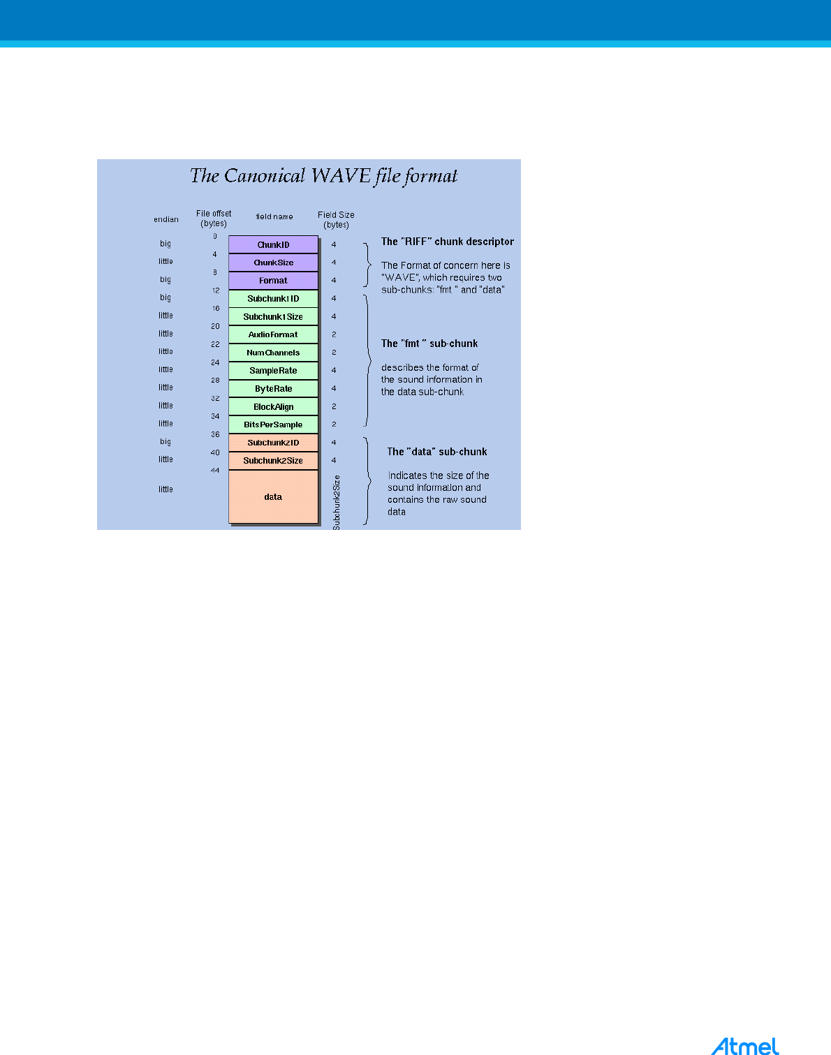
In this case, the timer is configured to operate in sample rate of the input .wav files retrieved from the WAVE
header of the file. A standard WAVE header is shown in Figure 3-6.
Figure 3-6. Standard WAVE File Format
More details of WAVE header is available at reference
[2]
. Figure 3-7 shows the application flow of the WAV
audio player.
AT11493: Waveform Generator and WAV Audio Player using DAC [APPLICATION NOTE]
Atmel-42458A-Waveform-Generator-and-WAV-Audio-Player-using-DAC_ApplicationNote_042015
1
1
11
Figure 3-7. Application Flow Diagram – WAV Audio Player
Apart from Timer, Event System, and DAC, SERCOM USART peripheral is also used in the application which
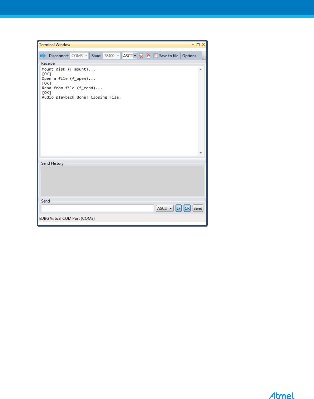
outputs the current status of FAT file system operations to the terminal window.
AT11493: Waveform Generator and WAV Audio Player using DAC [APPLICATION NOTE]
Atmel-42458A-Waveform-Generator-and-WAV-Audio-Player-using-DAC_ApplicationNote_042015
1
2
12
Figure 3-8. Terminal Window Showing SD/FATFS Operation Status
The clock flow for WAV audio player follows the same clock flow as waveform generator application.
3.2.2 Getting Started
Open the example project “DAC WAV Audio Player’ – SAM D20 Xplained Pro” in ‘Atmel Studio → File → New
→ Example Project”. The generated project directory has two .wav files one with 8kHz sample rate and one
with 16kHz sample rate. These files should be first copied to a microSD card using a card reader or similar.
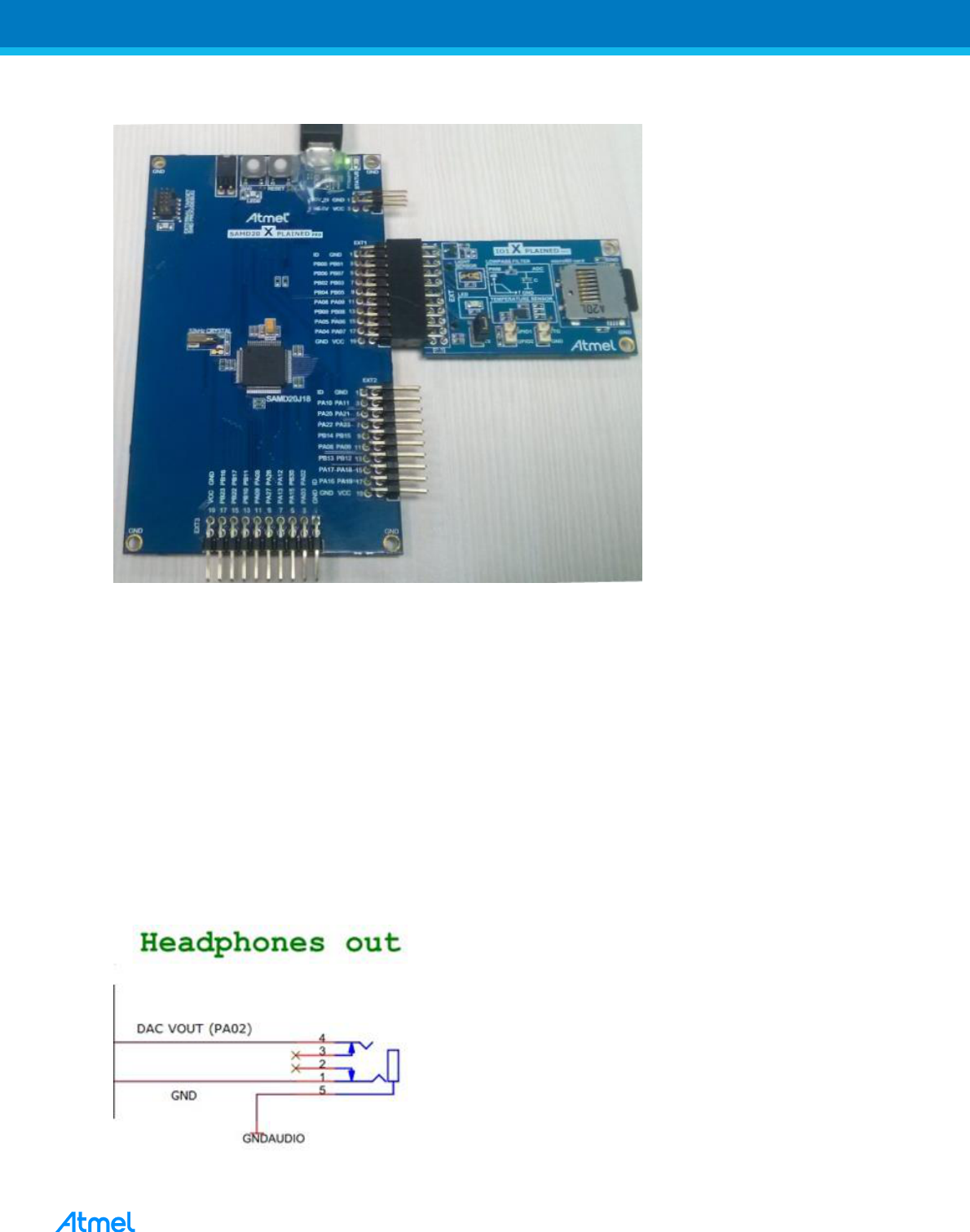
The microSD card should be now plugged into I/O1 Xplained Pro board which should be then connected to the
EXT1 header in the SAM D20 Xplained Pro board as shown in Figure 3-9.
AT11493: Waveform Generator and WAV Audio Player using DAC [APPLICATION NOTE]
Atmel-42458A-Waveform-Generator-and-WAV-Audio-Player-using-DAC_ApplicationNote_042015
1
3
13
Figure 3-9. SAM D20 Xplained Pro Board with I/O1 Xplained Pro
Open the file main.c and modify the following filename string definition which specifies the .wav filename in the
microSD card.
char test_file_name[] = "test_16khz.wav";
Now save the file, right click on ‘WAV_Player’ and click ‘Build’ which builds the project. Start the debug session
and run the project.
The audio output will be available on pin PA02 in EXT3 header in SAM D20 Xplained Pro board. Pin PA02 and
ground signal can be connected to an external audio amplifier with speaker system to verify the output. The
very simple way to verify the output is to connect the PA02 output and ground signal to a 3.5mm audio jack
and audio can be listened through headphones as shown in Figure 3-10.
Figure 3-10. DAC Output Connection to 3.5mm Audio Jack

AT11493: Waveform Generator and WAV Audio Player using DAC [APPLICATION NOTE]
Atmel-42458A-Waveform-Generator-and-WAV-Audio-Player-using-DAC_ApplicationNote_042015
1
4
14
3.2.3 Application Limitations
The WAV player application implemented as a part of this application note is a reference implementation
demonstrating the usage of DAC module. Following are the .wav file audio specification with which the
application has been tested.
1. Sample Rate – 8kHz and 16kHz.
2. Audio channels – Stereo (two channels).
3. Bit resolution – 16-bit signed PCM.
Files with audio specification other than listed above might not work with this application.
Note: Only left channel samples of the stereo input is processed and fed to DAC for playback. The
application will not perform an average of left and right channels for playback.
4 References
[1] SAM D20 Device Datasheet
[2] Microsoft
®
WAV File Format
[3] I/O1 Xplained Pro
[4] SAM D20 Xplained Pro

AT11493: Waveform Generator and WAV Audio Player using DAC [APPLICATION NOTE]
Atmel-42458A-Waveform-Generator-and-WAV-Audio-Player-using-DAC_ApplicationNote_042015
1
5
15
5 Revision History
Doc Rev.
Date
Comments
42458A
04/2015
Initial document release.

AT11493: Waveform Generator and WAV Audio Player using DAC [APPLICATION NOTE]
Atmel-42458A-Waveform-Generator-and-WAV-Audio-Player-using-DAC_ApplicationNote_042015
1
6
16
Atmel Corporation 1600 Technology Drive, San Jose, CA 95110 USA T: (+1)(408) 441.0311 F: (+1)(408) 436.4200 │ www.atmel.com
© 2015 Atmel Corporation. / Rev.:Atmel-42458A-Waveform-Generator-and-WAV-Audio-Player-using-DAC_ApplicationNote_042015.
Atmel
®
, Atmel logo and combinations thereof, Enabling Unlimited Possibilities
®
, and others are registered trademarks or trademarks of Atmel Corporation in U.S. and
other countries. Microsoft
®
is a registered trademark of Microsoft Corporation in U.S. and or other countries. Other terms and product names may be trademarks of
others.
DISCLAIMER: The information in this document is provided in connection with Atmel products. No license, express or implied, by estoppel or otherwise, to any intellectual property right
is granted by this document or in connection with the sale of Atmel products. EXCEPT AS SET FORTH IN THE ATMEL TERMS AND CONDITIONS OF SALES LOCATED ON THE
ATMEL WEBSITE, ATMEL ASSUMES NO LIABILITY WHATSOEVER AND DISCLAIMS ANY EXPRESS, IMPLIED OR STATUTORY WARRANTY RELATING TO ITS PRODUCTS
INCLUDING, BUT NOT LIMITED TO, THE IMPLIED WARRANTY OF MERCHANTABILITY, FITNESS FOR A PARTICULAR PURPOSE, OR NON-INFRINGEMENT. IN NO EVENT
SHALL ATMEL BE LIABLE FOR ANY DIRECT, INDIRECT, CONSEQUENTIAL, PUNITIVE, SPECIAL OR INCIDENTAL DAMAGES (INCLUDING, WITHOUT LI MITATION, DAMAGES
FOR LOSS AND PROFITS, BUSINESS INTERRUPTION, OR LOSS OF INFORMATION) ARISING OUT OF THE USE OR INABILITY TO USE THIS DOCUMENT, EVEN IF ATMEL
HAS BEEN ADVISED OF THE POSSIBILITY OF SUCH DAMAGES. Atmel makes no representations or warranties with respect to the accuracy or completeness of the contents of this
document and reserves the right to make changes to specifications and products descriptions at any time without notice. Atmel does not make any commitment to update the information
contained herein. Unless specifically provided otherwise, Atmel products are not suitable for, and shall not be used in, automotive applications. Atmel products are not intended,
authorized, or warranted for use as components in applications intended to support or sustain life.
SAFETY-CRITICAL, MILITARY, AND AUTOMOTIVE APPLICATIONS DISCLAIMER: Atmel products are not designed for and will not be used in connection with any applications where
the failure of such products would reasonably be expected to result in significant personal injury or death (“Safety-Critical Applications”) without an Atmel officer's specific written consent.
Safety-Critical Applications include, without limitation, life support devices and systems, equipment or systems for the operation o f nuclear facilities and weapons systems. Atmel
products are not designed nor intended for use in military or aerospace applications or environments unless specifically designated by Atmel as military-grade. Atmel products are not
designed nor intended for use in automotive applications unless specifically designated by Atmel as automotive-grade.
